
Executive Summary
- Domestic fab buildout is real but pre-commercial: TSMC’s Fab 21 in Phoenix achieved high-volume 4nm production in 2026, anchored by a $6.6 billion CHIPS Act award, with a second 2nm facility completing construction in April 2026. By 2032, the U.S. is projected to hold 28% of global advanced logic capacity, up from near-zero in 2022 — a structural shift, though full production benefit remains 18–36 months out per fab cycle.
- Advanced packaging, not wafer starts, is the binding supply constraint: TSMC’s CoWoS capacity is scaling from roughly 35,000 to 130,000 wafers per month by end-2026, yet demand continues to outpace supply. NVIDIA absorbs an estimated 60%-plus of current CoWoS allocation, creating severe rationing pressure on non-hyperscaler customers through at least 2027.
- HBM memory is in a structural supercycle with dangerous concentration: HBM demand grew 130% year-on-year in 2025 and is forecast to grow a further 70% in 2026. SK Hynix holds 62% global HBM market share, with Samsung and Micron competing for the remainder. Supply shortages are projected to persist through 2027, creating a DRAM diversion effect that tightens the broader memory market.
- China’s rare earth leverage is asymmetric and durable: The April 2025 Chinese export licensing regime on seven medium and heavy rare earths remains fully in force as of May 2026. Beijing’s December 2024 prohibition on gallium and germanium exports — covering a commodity China controls at roughly 98% of global refined supply — was partially suspended in November 2025 but is subject to review in late 2026. This leverage is structural, not transitory.
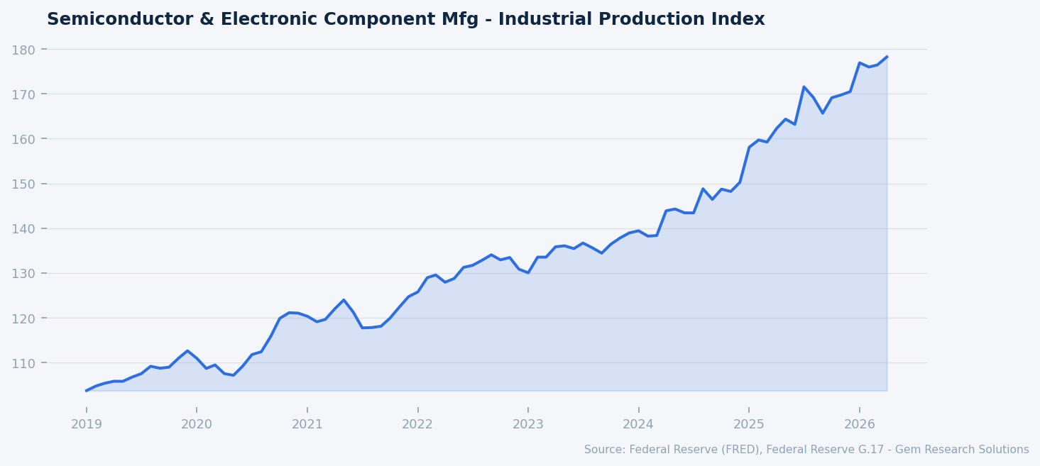
Semiconductor & electronic component manufacturing — industrial production index. Source: FRED.
Market Overview
Global semiconductor supply chains in 2026 are operating under a dual tension: material resilience gains accumulated since the 2021–2022 shortage era are now visible in production metrics, while new and deeper structural vulnerabilities have emerged at the advanced packaging, memory, and critical minerals layers. The industrial picture is nuanced. As of Q1 2026, U.S. manufacturing capacity utilisation stood at 75.7%, fractionally below the long-run average of 76.0%, per Federal Reserve data — a reading that masks significant variation across semiconductor subsectors where utilisation of leading-edge capacity is effectively at ceiling while trailing-edge capacity remains partially idle. The Semiconductor IP Index reached 178.2 as of May 2026, versus approximately 105 in 2019, reflecting the sustained capital intensity of the current investment cycle. U.S. private nonresidential fixed investment is running at $3.8 trillion SAAR, per Bureau of Economic Analysis data, with semiconductor-related construction and equipment representing one of the fastest-growing components.
The macro environment frames the analysis in important ways. The Federal Reserve’s benchmark rate stands at 3.64% following a measured easing cycle from the 2023 peak, reducing the financing cost pressure on multi-year fab construction projects. The 10-year Treasury at 4.48% and the 10Y-2Y yield spread at +46 basis points — fully unwound from its -108 basis point inversion peak in 2023, per Federal Reserve data — signal that financial conditions, while not accommodative, are supportive of long-dated capital investment. The VIX at 16.3 indicates a low-volatility market environment, consistent with sustained institutional appetite for semiconductor equity and credit. High-yield option-adjusted spreads of 271 basis points and investment-grade spreads of 74 basis points, both materially tighter than period averages per FRED, suggest that debt financing for capacity expansion projects remains accessible for investment-grade issuers.
The geopolitical overlay has hardened meaningfully since 2024. The U.S.-China technology confrontation is no longer a bilateral negotiating exercise but a multi-front structural divergence involving export controls, rare earth supply leverage, and parallel industrial policy programs on both sides. Against this backdrop, resilience in semiconductor supply chains must be measured not merely by inventory levels or lead times but by the durability of key input sources, the depth of advanced packaging capacity, and the speed at which domestic production ecosystems can achieve meaningful yield rates. On each of these dimensions, the gap between announced intent and operational reality remains wide.
CHIPS Act and the U.S. Fab Buildout: Transition from Subsidy to Production
The CHIPS and Science Act, signed in August 2022, committed $52.7 billion in federal funding to domestic semiconductor manufacturing, with the underlying thesis that U.S. geopolitical security required supply chains less exposed to concentration in Taiwan and East Asia. By 2026, that program has moved decisively from announcement to early production — but the gap between current output and the scale required for genuine supply independence remains substantial.
TSMC’s Fab 21 in Phoenix represents the most consequential single data point. The facility is now in high-volume production at the 4-nanometer node, supported by a $6.6 billion direct funding award from the CHIPS Act. In March 2025, TSMC committed an additional $100 billion to Arizona, encompassing three further advanced fabs, two packaging facilities, and a dedicated research and development center — bringing total Arizona investment commitments to $165 billion. The second fab, targeting 2-nanometer nanosheet technology, completed construction in April 2026. Commercial production is expected to begin in the second half of 2027. By 2032, according to projections cited by the Semiconductor Industry Association, the United States is expected to account for 28% of global advanced logic chip production, up from a position of near-zero just four years earlier.
Intel and Samsung are also hitting CHIPS Act programmatic milestones, making 2026 the year in which the transition from subsidy announcement to actual production ramp becomes observable in factory-level output data. The Semiconductor IP Index reading of 178.2, compared to approximately 105 in 2019, is a measurable indicator of the sustained investment cycle underway, per FRED data. However, this optimism must be tempered by structural constraints that are not addressable through capital alone. Workforce development pipelines for advanced semiconductor engineering remain a limiting factor. The 18–36 month lag between capex commitment and production output means the full benefit of current investment will not be felt in supply chain terms until 2028 at the earliest for most projects. Domestic equipment and materials ecosystems — photoresists, process chemicals, precision tooling — remain heavily import-dependent. Reshoring is a directional shift, not a near-term operational fix.
The 2nm production ramp at TSMC Arizona in 2027–2028 represents the first genuine test of whether U.S. talent depth and supplier ecosystems can sustain leading-edge yields at commercial scale. Yield rates at advanced nodes are highly sensitive to process control and supplier quality, and Taiwan’s decades of accumulated ecosystem density cannot be replicated by infrastructure investment alone. Gem Research considers this yield execution risk as the single most important watch item in the domestic fab buildout narrative over the next 24 months.
Advanced Packaging: CoWoS as the Proximate AI Infrastructure Constraint
The conventional framing of semiconductor supply risk focuses on wafer starts and node geometry — how many chips can be manufactured at leading-edge nodes, and where. That framing is now materially incomplete. The binding constraint on AI infrastructure buildout in 2026 is not wafer production capacity but advanced packaging, and specifically Chip-on-Wafer-on-Substrate technology, known as CoWoS, which enables the high-bandwidth integration of logic and memory dies required by the latest generation of AI accelerators.
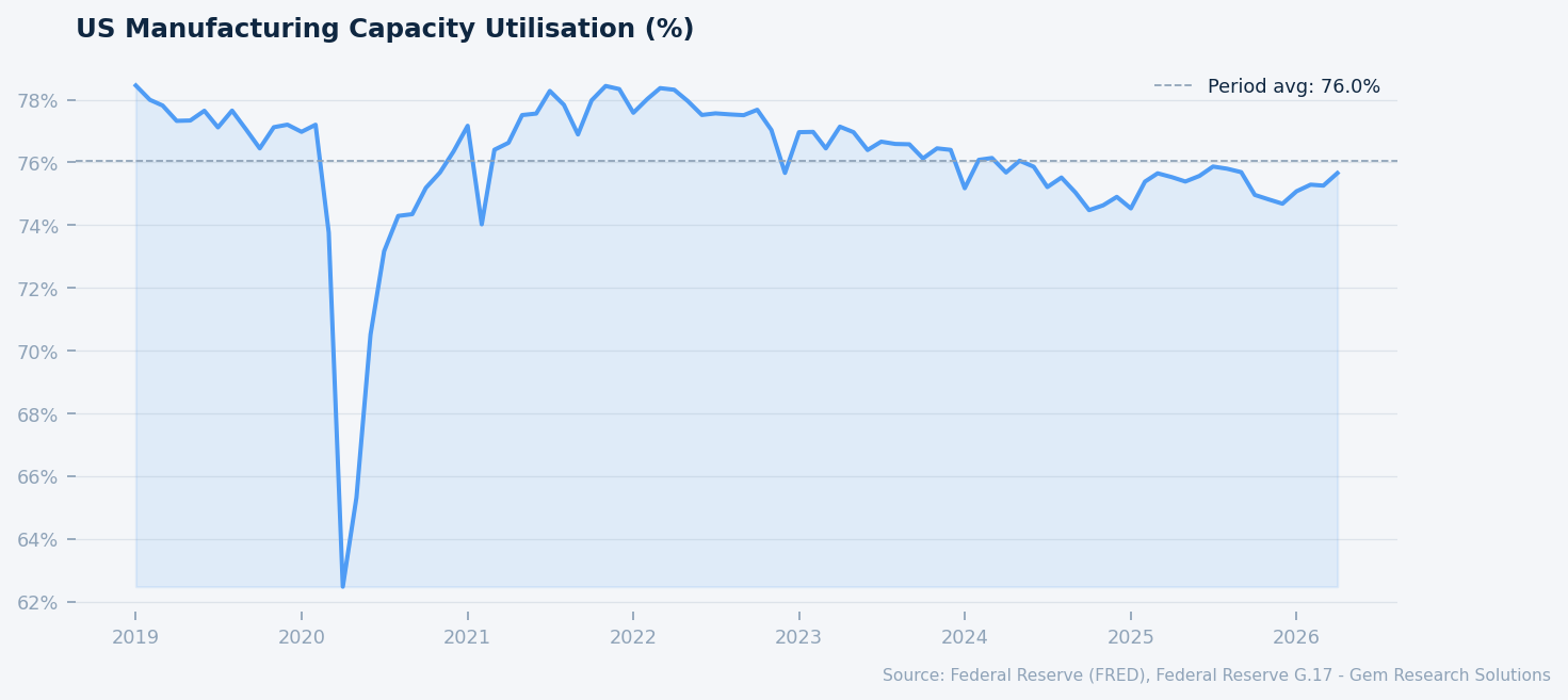
US manufacturing capacity utilisation (%). Source: FRED, Federal Reserve G.17.
TSMC’s CoWoS capacity is scaling aggressively, from roughly 35,000 wafers per month in late 2024 to a projected 130,000 wafers per month by end-2026. That near-fourfold increase in capacity represents a significant operational achievement. Yet TSMC’s own chief executive has confirmed that CoWoS capacity remains sold out through 2025 and into 2026, and the demand trajectory from hyperscalers continues to outrun supply additions. NVIDIA alone commands over 60% of current CoWoS allocation, absorbing an estimated 595,000 wafers in 2026 for its Rubin architecture. The concentration of this allocation in a single customer creates a structurally adverse position for the remainder of the customer base: non-NVIDIA firms seeking CoWoS capacity face severe rationing and multi-quarter lead times, effectively constraining their AI product development cycles regardless of their own design capabilities.
TSMC has begun outsourcing packaging steps to ASE Technology and Amkor Technology to expand effective system capacity. ASE projects its advanced packaging revenue to double in 2026, a figure that reflects both genuine demand growth and the structural elevation of packaging firms from commodity assemblers to systemically important supply chain nodes. For investors and procurement officers alike, packaging capacity has become a strategic variable that demands the same analytical attention previously reserved for leading-edge foundry capacity.
The CoWoS bottleneck is not expected to clear before 2027 at the earliest, and even then, demand growth assumptions embedded in hyperscaler capital expenditure plans suggest continued tightness. U.S. private nonresidential fixed investment running at $3.8 trillion SAAR, per Bureau of Economic Analysis data, includes substantial AI data center buildout, the majority of which depends on CoWoS-packaged chips. Supply constraints at the packaging layer therefore translate directly into data center commissioning delays and AI infrastructure cost escalation — a linkage that has not yet been fully priced into consensus capital expenditure forecasts.
HBM Memory: Supercycle Dynamics and Structural Concentration Risk
High Bandwidth Memory has become the third critical chokepoint in the AI semiconductor supply chain, alongside leading-edge logic capacity and advanced packaging. HBM demand grew 130% year-on-year in 2025 and is forecast to grow a further 70% in 2026, according to Bank of America research, which characterises the current environment as a DRAM supercycle — a designation that carries significant historical weight given the cyclicality that has characterised the memory industry over the past three decades. Bank of America projects global DRAM revenue growth of 51% year-on-year in 2026, a figure that reflects both HBM volume growth and the price dynamics created by wafer reallocation from conventional DRAM to HBM production.
SK Hynix holds approximately 62% of the global HBM market as of Q2 2025, a position secured through early and exclusive supply agreements with NVIDIA for HBM3E memory used in H100 and H200 GPU systems. That first-mover advantage has translated into a durable market position that competitors are only beginning to challenge at scale. Samsung, holding approximately 17% market share, completed HBM3E qualification in 2025 and is now ramping mass production. Micron, at approximately 21% share, is shipping 12-stack HBM3E from facilities in New York and Idaho, with SK Hynix’s Indiana packaging plant adding a U.S.-based node to the supply chain for the first time. Both Samsung and SK Hynix have issued guidance suggesting that supply shortages in HBM could persist through 2027 and beyond, with major customers reserving capacity through multi-year forward agreements.
The DRAM diversion effect deserves particular analytical emphasis. Wafers reallocated to HBM production are unavailable for conventional DRAM manufacturing. As AI infrastructure demand continues to pull HBM capacity, the supply of standard DRAM for PC, server, and mobile applications tightens simultaneously — creating a cross-market pricing effect that benefits all DRAM producers but particularly burdens buyers in non-AI segments. China’s CXMT is pursuing HBM3E capability, but access to advanced extreme ultraviolet lithography equipment remains blocked by U.S. and allied export controls, limiting its competitive relevance to the domestic Chinese market in the medium term.
China Export Controls and Rare Earth Leverage
The material escalation in the U.S.-China technology confrontation since late 2024 has introduced a category of supply risk that differs qualitatively from the capacity and packaging constraints discussed above: it is geopolitically determined, not commercially resolvable, and subject to reversal only through diplomatic negotiation rather than investment or engineering. This distinction matters for risk management frameworks at both the corporate and sovereign levels.
In December 2024, China issued an outright prohibition on exports of gallium, germanium, antimony, and superhard materials to the United States — an escalation from the licensing requirements that had been in place since 2023. China controls approximately 98% of global refined gallium supply, which is a critical input for compound semiconductors deployed in 5G communications, radar systems, and satellite infrastructure. The prohibition represents a significant shift from leverage to active denial. In April 2025, Beijing expanded its export control regime to include seven medium and heavy rare earth elements — terbium, dysprosium, samarium, gadolinium, lutetium, scandium, and yttrium — directly targeting magnet production inputs essential to both chipmaking equipment and advanced defense systems.
In November 2025, China partially suspended the October 2024 escalation for a period of one year and restored standard licensing procedures for gallium, germanium, and antimony. However, the April 2025 rare earth licensing regime was explicitly not suspended and remains fully in force as of May 2026. A TechTimes report dated May 26, 2026 confirms these curbs continue to constrain supply chains, with a formal U.S.-China review of the control framework expected in late 2026. The asymmetry is clear: China’s partial concession on industrial metals was tactical and time-limited, while the rare earth licensing regime is structural and has no announced sunset date. Western defense and semiconductor manufacturers face a durable input-cost and availability risk with no near-term commercial substitute.
On the U.S. side, export controls carry their own cost. Analysis from the Information Technology and Innovation Foundation estimates that full decoupling from China would cost U.S. semiconductor firms $77 billion in first-year revenue, reduce industry R&D by 24% — approximately $14 billion — and eliminate 80,000 direct and 500,000 downstream jobs. NVIDIA absorbed a $5.5 billion charge in 2025 from export restrictions; AMD recorded an $800 million impact. These are not hypothetical costs — they are visible in reported financials.
Risk Factors
Rare Earth Supply Disruption Escalation. The April 2025 Chinese licensing regime on seven medium and heavy rare earths remains in force with no sunset provision. Should Beijing tighten enforcement, restrict quota issuance, or expand the prohibited materials list in response to further U.S. export control actions, Western semiconductor equipment manufacturers and defense prime contractors face genuine input shortages with no commercially viable substitute supply available at scale within a 12–24 month horizon. The late 2026 U.S.-China review of the one-year gallium/germanium suspension is the proximate catalyst to watch. An unfavorable outcome — non-renewal of the suspension — would immediately re-tighten industrial metal availability and amplify cost pressures across compound semiconductor applications.
CoWoS Demand Overshoot and Hyperscaler Capex Correction. Current CoWoS capacity expansion plans are calibrated to hyperscaler AI capex projections that assume continued strong AI infrastructure investment through 2027 and beyond. If AI workload growth disappoints relative to infrastructure buildout — a risk that has precedent in prior technology investment cycles — a demand correction could leave TSMC and its packaging subcontractors with capacity built to a demand curve that has shifted. The tightness of current high-yield credit spreads, at 271 basis points versus a period average of approximately 330 basis points per FRED data, suggests markets are not pricing meaningful tail risk in this scenario.
U.S. Fab Yield Execution Risk. The 2nm production ramp at TSMC Arizona, targeted for H2 2027, carries material yield uncertainty. Advanced node yields are highly sensitive to process control, materials quality, and supplier ecosystem depth. Any significant yield underperformance relative to Taiwan benchmarks would delay the U.S. share gain in advanced logic capacity, extend dependence on Taiwan-based production, and raise the effective per-chip cost of domestically sourced semiconductors — with direct implications for AI accelerator pricing and U.S. defense procurement programs.
Gem Research Perspective
Gem Research’s analytical call on semiconductor supply chains in 2026 is one of differentiated resilience: progress is real at the system level, but the chain of constraints has migrated rather than resolved. The 2021–2022 era shortage, driven by demand surge and legacy-node underinvestment, has given way to a new supply architecture in which advanced packaging and specialized memory have displaced wafer production as the primary bottlenecks. The structural consequence is that companies positioned across the CoWoS and HBM supply chain — TSMC’s packaging operations, ASE, Amkor, SK Hynix, and Micron — hold more pricing power and strategic leverage than leading-edge wafer fabs alone would suggest.
The China rare earth dimension is the variable we weight most heavily as a source of unpriced risk. The April 2025 licensing regime is permanent-until-revoked, and Beijing has demonstrated both the capability and the political will to use materials leverage as a negotiating instrument. Western governments have not yet built diversified rare earth refining capacity at the scale required to materially reduce this dependence within a five-year horizon. We expect this risk to remain structurally unresolved through at least 2028.
We recommend that analysts and institutional clients track three leading indicators over the next four quarters: CoWoS wafer allocation data in TSMC quarterly disclosures; the outcome of the late 2026 U.S.-China rare earth control review; and initial yield reports from TSMC Arizona’s 2nm ramp. These three data points will determine whether the resilience narrative of 2026 is validated or revised materially downward.